|
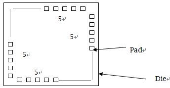
1) Creating the device parameter Create each set up elements such as device name, wafer size, XY indexing size, OF direction, chuck temperature, multi measuring and needle height of the card. 2) Setting of operation parameter Set up needle position alignment (manual), needle height (manual) and standard of XY coordinator. 3) Stop prober before probing and load the wafer. Measure the center of wafer thickness automatically. 4) Alignment Registration Register the street junction,  Select alignment references at low and high magnification. The points to select the reference Pattern which has clear contrast Place where vertical and horizontal lines are clear Unique location Do not register when there is a TEG in a street, or do not register the TEG die. Avoid the pad, which is for high magnification only. (It starts the alignment automatically when the registration completes) 4) Pad Registration  Register 16~20 corner pads in total.  (It starts needle alignment automatically when the pad registration completes) 5) Create and revise the map (Able to revise by comparing with the image of the chip) 6) Save newly created device to HD Continue to make sure contact height >> Start probing |


